|
Shen Zhen Hongfu Hua Technology Co., Ltd.
|
Gold Index: 8100


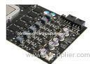
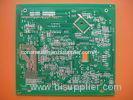
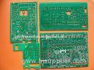
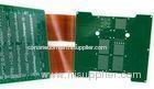
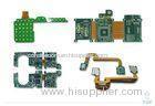
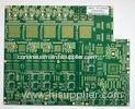
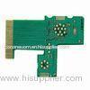
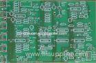
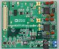
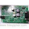
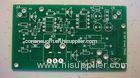
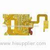
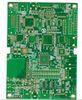
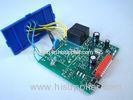
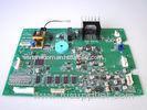
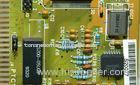
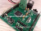
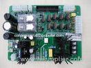
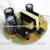
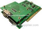
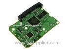
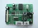
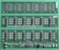
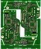
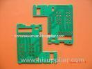
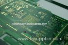
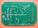
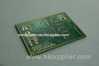
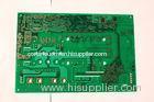
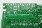
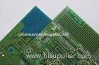
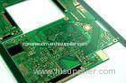
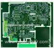
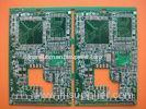
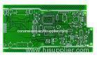
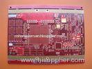
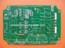
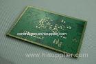
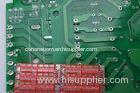
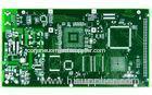
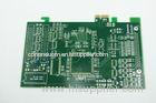
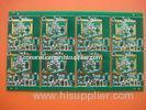
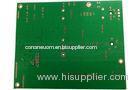
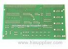
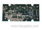
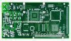
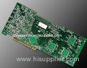
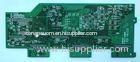
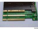
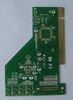
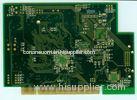
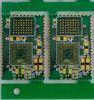
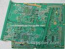
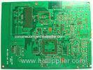
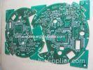
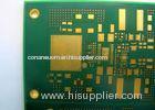
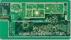
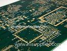
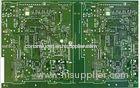
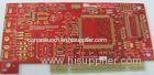
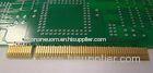
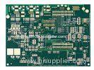
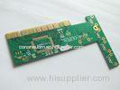
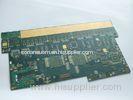
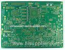
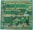
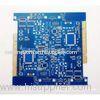
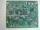
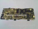
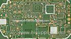
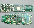
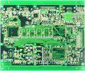
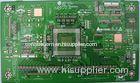
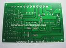
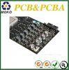
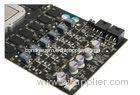
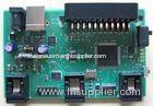
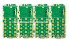
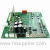
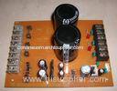
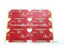
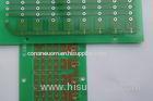
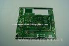
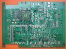
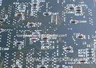
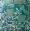
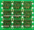
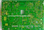
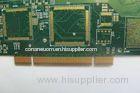
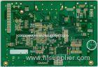
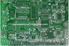
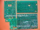
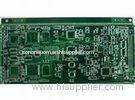
4-Layer rigid flex pcb for cell phone pcb Green / Blue Solder mask ENIG finish
| Place of Origin: | Zhejiang, China (Mainland) |
|
|
|
| Add to My Favorites | |
| HiSupplier Escrow |
Product Detail
4-Layer rigid flex pcb for cell phone pcb Green / Blue Solder mask ENIG finish
Quick Details
4-Layer rigid flex pcb for cell phone pcb Green / Blue Solder mask ENIG finish
Quick Details
| Place of Origin: | China (Mainland) | Brand Name: | OEM | Model Number: | H015K |
| Number of Layers: | 4-Layer | Base Material: | PI | Copper Thickness: | 1OZ |
| Board Thickness: | 1.6mm | Min. Hole Size: | 0.2mm | Min. Line Width: | 0.1mm |
| Min. Line Spacing: | 0.1mm | Surface Finishing: | ENIG | Solder mask: |
Green/Blue/Black/White/Yellow/Red etc
|
| Max size of finish board: | 9200*900mm | Certification: | UL/SGS/ROHS | Controlled impedance: | ±5% |
| Warp&Twist: | 0.7% | Rang of finish boards thickness: | 0.21~7.0mm | Layer count: | 1~28 |
| Impedance control: | ±10% | OEM/ODM: | One-stop service | PCB standard: | IPC-A-610D |
Specifications
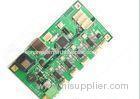
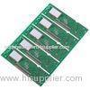
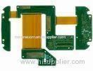
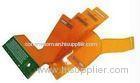
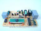
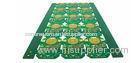
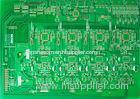
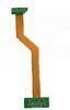
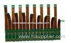
rigid flex pcb
a.PCB OEM&ODM Clone/Copy
b.PCB Design
c.Turnkey service
d.UL,SGS,RoSH,TS
rigid flex pcb
1.ENIG finish required to meet ROHS compliant;
2.PI material within 0.2mm-3.2mm boards thickness;
3.Copper weight:0.5OZ,1OZ,2OZ,3OZ;
4.0.2mm min finished hole size;
5.Certificate: UL, ROHS, T/S16949;
6.Company management: ISO9001:2000;
7.Markets: Europe, America, Asia etc all over the world.
PCB manufacturing capacity
|
NO |
Item |
Craft Capacity |
|
1 |
Layer |
1-28 Layers |
|
2 |
Base Material for PCB |
FR4, CEM-1, TACONIC, Aluminium, High Tg Material, High Frequence ROGERS , TEFLON, ARLON, Halogen-free Material |
|
3 |
Rang of finish baords Thickness |
0.21-7.0mm |
|
4 |
Max size of finish board |
900MM*900MM |
|
5 |
Minimum Linewidth |
3mil (0.075mm) |
|
6 |
Minimum Line space |
3mil (0.075mm) |
|
7 |
Min space between pad to pad |
3mil (0.075mm) |
|
8 |
Minimum hole diameter |
0.10 mm |
|
9 |
Min bonding pad diameter |
10mil |
|
10 |
Max proportion of drilling hole and board thickness |
1:12.5 |
|
11 |
Minimum linewidth of Idents |
4mil |
|
12 |
Min Height of Idents |
25mil |
|
13 |
Finishing Treatment |
HASL (Tin-Lead Free), ENIG(Immersion Gold), Immersion Silver , Gold Plating (Flash Gold), OSP, etc. |
|
14 |
Soldermask |
Green, White, Red, Yellow, Black, Blue, transparent photosensitive soldermask, Strippable soldermask. |
|
15 |
Minimun thickness of soldermask |
10um |
|
16 |
Color of silk-screen |
White, Black, Yellow ect. |
|
17 |
E-Testing |
100% E-Testing (High Voltage Testing); Flying Probe Testing |
|
18 |
Other test |
ImpedanceTesting,Resistance Testing, Microsection etc., |
|
19 |
Date file format |
GERBER FILE and DRILLING FILE, PROTEL SERIES, PADS2000 SERIES, Powerpcb SERIES, ODB++ |
|
20 |
Special technological requirement |
Blind & Buried Vias and High Thickness copper |
|
21 |
Thickness of Copper |
0.5-14oz (18-490um) |
Related Search
Find more related products in following catalogs on Hisupplier.com
Company Info
Shen Zhen Hongfu Hua Technology Co., Ltd. [China (Mainland)]
Business Type:Manufacturer
City: Shenzhen
Province/State: Guangdong
Country/Region: China (Mainland)